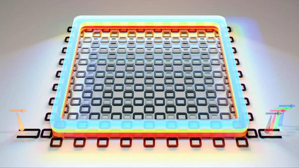
Researchers at the Joint Quantum Institute (JQI) have developed a novel photonic chip capable of converting a single input laser frequency into multiple distinct output colors—specifically generating second, third and fourth‐harmonic frequencies—without requiring any active tuning or embedded heaters. This is achieved through a clever micro-resonator array structure featuring dual timescales (fast individual rings plus a slower “super‐ring”) that inherently satisfies the frequency–phase matching conditions normally achieved only with painstaking design or active compensation. The advance promises to streamline and miniaturize components for integrated photonics, enhancing technologies such as quantum computing, precision metrology and multi-wavelength communications.
Key Takeaways
– The chip design uses an array of micro-resonators operating at two distinct timescales to passively satisfy frequency–phase matching and reliably generate multiple harmonics.
– Eliminating the need for active tuning (e.g., embedded heaters) simplifies the fabrication and enhances reproducibility for integrated photonic devices.
– The technology has broad implications for high‐precision measurement (metrology), quantum computing, and advanced communication systems by enabling compact, multi-wavelength light sources.
In-Depth
The demand for compact, efficient photonic devices that integrate seamlessly into chip-scale platforms continues to rise—driven by applications in quantum computing, high-speed data communications and precision measurement systems. A recent breakthrough from the Joint Quantum Institute (JQI) offers a major step forward in this arena by demonstrating a photonic chip that passively converts a single laser input into multiple output frequencies without any active tuning mechanisms. Traditional approaches to frequency conversion on chip often required carefully tuned resonators with embedded heaters or other active compensation to ensure matching between the fundamental and harmonic frequencies; even small fabrication variations could throw off the delicate balance and reduce yield or consistency. The new design sidesteps these challenges by leveraging an array of micro-ring resonators arranged such that light circulates through both “fast” rings and a slower “super-ring” structure. This dual-timescale circulation inherently improves the chances of satisfying both frequency and phase‐matching conditions simultaneously, enabling the chip to efficiently generate second, third and fourth harmonics of an input laser (~190 THz in the demonstrated case) and output distinct colors (e.g., red, green, blue) without any active compensation.
By removing the requirement for active tuning, this approach enhances reproducibility and manufacturability—key considerations as photonic devices move from laboratory prototypes toward scalable production. The ability to embed multiple wavelengths on a chip is particularly significant for applications like wavelength-division multiplexing in fiber optics, integrated quantum systems where different qubit wavelengths must be converted or routed, and high-precision metrology where optical signals at multiple harmonics allow enhanced sensing or timing measurements. Moreover, the fact that this design works across multiple chips on the same wafer enhances its practicality for commercial deployment. From a conservative‐leaning engineering and industry standpoint, this development offers an appealing combination of technical innovation and manufacturing pragmatism: an architecture that improves yield, reduces complexity (fewer active tuning components) and opens the door for multi-color light-source chips that can be integrated into existing photonic and electronic infrastructure. Over time, as demand for photonic integration grows—driven by data-center bandwidth needs, quantum computing deployments, lidar/optical sensing systems and more—technologies like this stand to contribute to improved performance, lower cost and smaller form-factors. That kind of-enabled flexibility aligns well with market realities and pragmatic engineering goals.
In sum, the JQI work on passively‐tuned harmonic conversion photonic chips represents a meaningful advance in integrated photonics. While the commercial timeline remains to be determined, the architecture addresses longstanding fabrication and tuning barriers, and positions multi-wavelength photonic chips for broader real-world deployment. If manufacturing scales and cost drivers follow, we may see applications ranging from dense optical communications inside data centers to compact quantum-sensor modules and even portable metrology tools leveraging multiple harmonics of light—all anchored by this more reliable chip design. As the industry transitions from electrons to photons (or complements them), innovations like this make that shift more practical and production-ready.


