

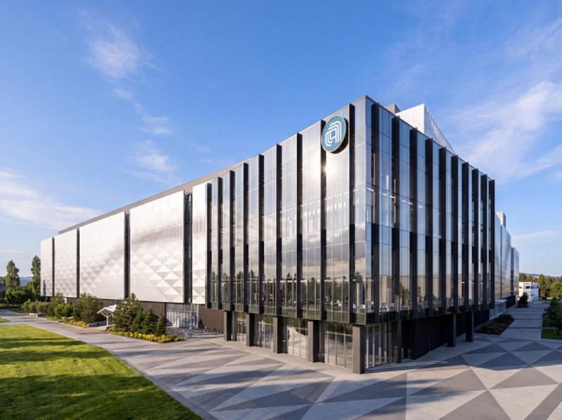
Applied Materials has unveiled its $5 billion Equipment and Process Innovation and Commercialization (EPIC) Center in Silicon Valley, establishing a major semiconductor research facility intended to accelerate the development of next-generation artificial intelligence chips. The 600,000-square-foot complex brings together leading semiconductor manufacturers, including Intel, Samsung, TSMC, Micron, and SK Hynix, alongside prominent research universities. Designed to eliminate costly delays between scientific discoveries and commercial production, the facility aims to shorten chip development cycles by at least 30% while advancing energy efficiency and manufacturing capabilities. The investment represents a significant private-sector commitment to American technological competitiveness as the United States confronts growing competition from China for leadership in artificial intelligence and semiconductor innovation.
Key Takeaways
• $5 Billion Investment: Applied Materials’ new 600,000-square-foot research center aims to accelerate semiconductor development and reduce the time required to bring advanced AI chips into commercial production.
• Industry Collaboration: Partnerships involving major chipmakers and American universities will integrate research, engineering, and manufacturing expertise to improve chip performance, energy efficiency, and production efficiency.
• American Technological Leadership: The investment strengthens domestic semiconductor research capabilities and could help the United States maintain its competitive advantage over China in artificial intelligence and advanced computing.
In-Depth
Applied Materials’ unveiling of its $5 billion semiconductor research center marks a significant development in America’s effort to maintain technological leadership in an increasingly competitive global economy. Located in Silicon Valley, the EPIC Center represents an ambitious private-sector investment in accelerating the production of advanced microchips essential to artificial intelligence, national security, and economic growth.
The 600,000-square-foot facility introduces a collaborative approach to semiconductor innovation, bringing manufacturers, equipment developers, and university researchers into a shared environment. Rather than developing technologies through traditionally separated research and manufacturing processes, participating organizations can coordinate their efforts earlier, potentially reducing development timelines by at least 30%.
Major semiconductor companies, including Intel, Samsung, TSMC, Micron, and SK Hynix, are participating in the broader initiative. Academic partnerships provide additional expertise in materials science, chip architecture, and manufacturing technologies. Together, these relationships could accelerate breakthroughs in computing performance while addressing the substantial electricity demands associated with expanding artificial intelligence infrastructure.
The investment also carries considerable strategic importance. Advanced semiconductors underpin military systems, communications networks, healthcare technologies, and virtually every major sector of the modern economy. America’s ability to develop these technologies domestically remains central to reducing vulnerabilities associated with international supply chains and intensifying Chinese competition.
Importantly, the initiative demonstrates how substantial private investment and cooperation between industry and academia can advance American innovation. Although research leadership alone cannot guarantee domestic manufacturing independence, shortening the path from laboratory discovery to commercial production offers a meaningful competitive advantage in an industry increasingly essential to national prosperity and security.